PhD Thesis
Modeling and Simulation of Negative Bias Temperature Instability
I completed my PhD thesis in 2007 at the Vienna University of Technology (TU Wien). It has since been published as a book and is available for purchase on Amazon. You can also find my Master’s thesis here.
Abstract
Semiconductor process and device simulators are well established tools for the reduction of the development time for semiconductor devices. Numerical simulation can help the device engineer to perform dozens of design experiments within the time normally needed to process one single wafer lot. Nowadays simulation efforts go beyond solving the basic semiconductor device equations. Especially the modeling and simulation of aging processes has tremendously gained in importance. This thesis tries to give insight into the topic of semiconductor device simulation and focuses on the modeling of degradation mechanisms.
After a first introduction, giving an overview of the motivation and the structure of this work, the fundamental equations for numerical device simulation, the modeling of generation and recombination mechanisms, as well as the modeling of quantum confinement effects are presented.
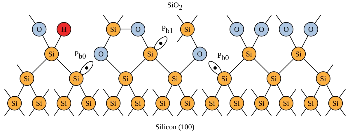
The possible defects at the Si/SiO2 interface are evaluated in the following chapter as this interface is of utmost importance in CMOS technology. An important topic is also the experimental characterization methods of the interface quality.
In the following a thorough investigation on degradation mechanisms affecting the gate dielectric is presented. These are the hot carrier degradation, dielectric wearout and breakdown, and the effect of quantum mechanical tunneling. Here, a new model is proposed for the numerical modeling of trap assisted tunneling currents across several electron traps.
The main part of this work concentrates on negative bias temperature instability (NBTI). NBTI causes degradation of MOS structures at elevated temperatures and negative gate voltages. An elaborate investigation of literature from the first report to the recent understanding of this degradation mechanism is presented. A comprehensive model is derived, combining research results from different groups and the coupling to the basic semiconductor device equations.
The new NBTI model is compared to measurement data and gives excellent results. Furthermore the susceptibility of CMOS circuits as the CMOS inverter, an SRAM cell, and a ring oscillator to NBTI is investigated in mixed mode device and circuit simulations. Stationary and transient simulations show the impact of degradation on real life circuits.